
 EN
EN
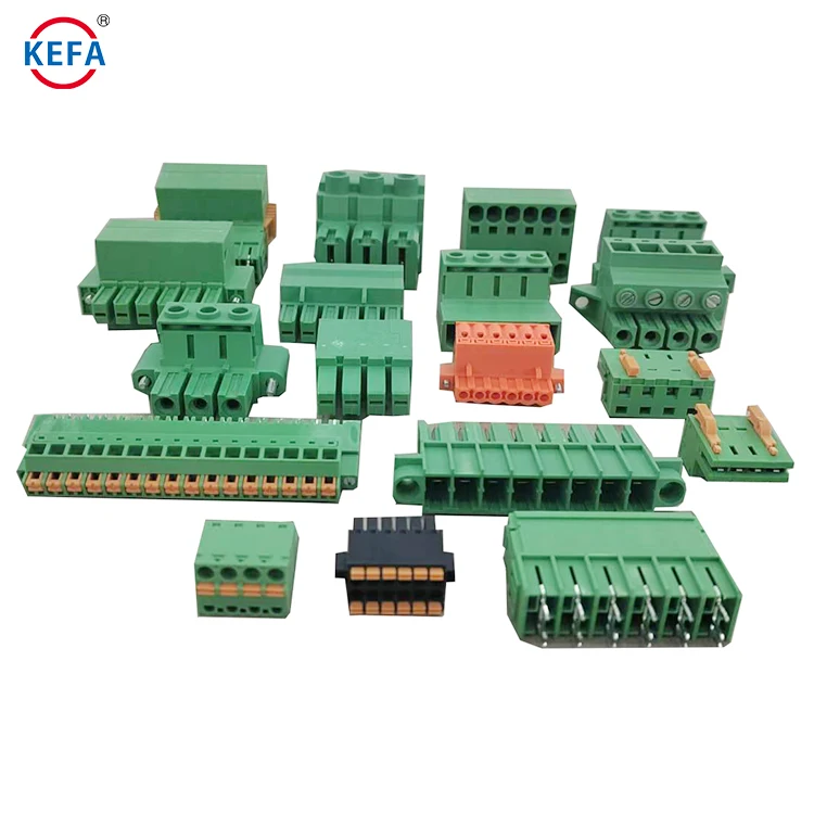
When designing a PCB (Printed Circuit Board), picking the correct connector footprint is really crucial. Connectors are those pieces that let different parts of a circuit board link up together. If the footprint, meaning the shape and size of the space for connector, isn't spot on, it might lead to issues such as poor links or damage on the board. At KEFA, we understands that solid design makes a huge impact on your project's success. This guide will show you how to select the proper PCB connector footprint and where to get resources to assist along the way.
How to Pick the Right PCB Connector Footprint for Your Project?
Selecting the right connector footprint is kind of like choosing shoes for a special occasion. Wrong size or type, and you end up with discomfort or odd appearance. So, first thing, figure out what connector type you need. There is many kinds, such as USB, HDMI, and power ones. Each have their own dimensions and form. You also should consider the pin count. More pins means more links, but it takes extra room too. Another key point is your PCB's arrangement. Make sure the footprint matches nicely with other parts on the board. Some are made for tight spots, while others require more area. It's wise to review the maker's specs. They gives detailed sizes and sketches to prevent errors. If unsure, check similar projects or get tips from pros. And finally, testing is essential. After drawing the footprint, build a test version and try it out for real. That way, you fix problems before the final build.
Where to Get Good Resources for PCB Connector Footprint Design?
Hunting for resources on PCB connectors footprints can seem like treasure hunt. But luckily, plenty places exist to check. Online groups and forums is great for advice from fellow designers. Sites with electronics tips and guides often offer free help. You can find software that makes designing footprints simpler. Some tools comes with libraries of standard footprints, which saves time and work. At KEFA, we offers support too for those seeking resources. Visit our site for design templates and advice. Books about PCB design are useful sources. They has best methods and samples to use. Don’t skip videos! Designers share tricks on YouTube, helpful if you learn by seeing. In addition, join local maker spots or electronics groups for practical learning from others. Remember, using more resources leads to better designs.
How to Optimize PCB Connector Footprint for Cheaper Making?
In designing a printed circuit board (PCB), the connector footprint play a big role. It's the area shape and size where connector sits on the PCB. To cut costs in production, optimize this footprint is key. Start by considering your connector's size. Ensure the footprint fits exact with its measurements. Too large or small, and assembly gets tricky. Good match means less errors and saves money. Also, look at how many connectors your board needs. Using fewer can lower expenses, since each connector cost something. That's why right number helps keep budget down.
Another tip for saving is sticking to standard connector sizes. Makers produce these common ones. By making your PCB for these standards, costs drop. Standard parts are usually cheaper and easier to get than custom. With this, think about PCB layout. Placing connectors nearer each other makes making simpler and less pricey. Closer means less material in the board. Also, keep traces – those connecting wires – as short as you can. Shorter ones is easier to produce and boosts circuit work.
Finally, use a solid service like KEFA for manufacturing. They has tools and know-how to optimize designs cheaply. Partnering with reliable ones ensures efficient and right connector making. This saves time and cash over time. Follow these, and your footprint will function well while being budget-friendly for needs.
What’s New in PCB Connector Footprint Design for Wholesalers?
Terminal PCB connector design world changes fast with trends. Wholesalers must keep up with latest in connector footprints to satisfy customers. One big trend is flexible footprints. This involve making them to handle various connector types. Rather than one specific for single connector, now they fit several. Such flex helps wholesalers provide more options without tons of different PCB layouts.
Another is tinier footprints. Tech gets smaller, so devices shrink too. Demand rises for compact connectors that save space. Wholesalers seek designs for these small ones. Tiny footprints makes products lighter and packs more features in less area. Customers like powerful, portable gadgets.
Sustainability gain traction too. Companies focus on green materials and ways. Designers aim to use less stuff but keep good performance. This could mean fewer layers in footprints or connectors needing less soldier. Wholesalers noting eco stuff can draw more green-seeking buyers.
Lastly, 3D printing shifts PCB designing. It lets quick prototypes. Designers test footprints fast and pick best. Wholesalers using it can launch products quicker. Staying ahead on trends means better offerings and edge over rivals.
Best Practices for Making PCB Connector Footprints?
Making a wire PCB connector footprint needs careful work and good habits. First, begin with precise measures of the connector. Use the datasheet from maker. It hold all key info, like hole sizes and pin gaps. Right sizes is vital for proper fit. Wrong footprint, and connector won't seat well, causing assembly troubles.
Next, consider layout. Arrange pins logical for the circuit. Minimize trace lengths from connector to other parts. Short traces cleans up design and cuts signal problems. When placing, leave enough room around. This eases soldering and avoids clashes with nearby components.
In addition, add clear labels on the design. Mark footprint so assemblers know exact spot. This reduces errors. Also, match your soldering method. For surface mount, design footprint accordingly.
Last, test always. Before finishing, prototype and try with real connectors. Spot issues early. At KEFA, we urges clients to do these checks. These practices lead to quality footprints that performs well for your project.
Table of Contents
- How to Pick the Right PCB Connector Footprint for Your Project?
- Where to Get Good Resources for PCB Connector Footprint Design?
- How to Optimize PCB Connector Footprint for Cheaper Making?
- What’s New in PCB Connector Footprint Design for Wholesalers?
- Best Practices for Making PCB Connector Footprints?